# Bragg mirrors and photonic crystals {#sec-bragg}
[](https://colab.research.google.com/github/{{< var github_user >}}/{{< var repo >}}/blob/main/{{< var subdir >}}/notebooks/bragg.ipynb){.colab-link} Run this chapter's code in Google Colab (no installation).
```{python}
#| include: false
import numpy as np
import matplotlib.pyplot as plt
import optolib as ol
ol.use_style()
c0, nm, um = ol.c0, ol.nm, ol.um
```
*Slides 176–190 (dielectric mirror, quarter-wave stack, reflectance versus number of pairs and index contrast, stop band,
penetration depth) and slides 289–294 (photonic crystals in 1D, 2D and 3D, band gaps, defects).*
## Key relations
A **dielectric (Bragg) mirror** stacks layers of alternating high ($n_1=n_H$) and low ($n_2=n_L$) index (slide 176). The reflection
coefficient changes sign at each interface, and with quarter-wave layers all reflected waves come back in phase (slide 177):
$$
n_1d_1+n_2d_2=\frac{\lambda}{2}\quad\Rightarrow\quad d_1=\frac{\lambda}{4n_1},\ d_2=\frac{\lambda}{4n_2}\qquad\text{(slides 181–182)}.
$$
| result | formula | slide |
|---|---|---|
| peak reflectance, $N$ pairs | $R_N=\left[\dfrac{n_0n_2^{2N}-n_3n_1^{2N}}{n_0n_2^{2N}+n_3n_1^{2N}}\right]^2$ | 179, 186 |
| stop-band width (infinite stack) | $\Delta\lambda\approx\dfrac{4\lambda_0}{\pi}\arcsin\!\left(\dfrac{n_1-n_2}{n_1+n_2}\right)$ | 179, 188 |
| penetration depth | $L_\text{pen}=-\dfrac12\dfrac{d\phi}{dk}$ of the reflection phase, $\approx\dfrac{\lambda}{4\Delta n}$ | 189 |
$R$ grows quickly with the number of pairs, and the bandwidth is set mainly by the index contrast (slides 184, 190).
### Bragg-mirror designer, live
```{ojs}
//| echo: false
viewof bm = Inputs.form({
  nH: Inputs.range([1.3, 4], {value: 2.49, step: 0.01, label: "high index n_H"}),
  nL: Inputs.range([1.0, 3.5], {value: 1.55, step: 0.01, label: "low index n_L"}),
  N:  Inputs.range([1, 30], {value: 4, step: 1, label: "number of pairs N"}),
  ns: Inputs.range([1, 4], {value: 1.47, step: 0.01, label: "substrate index n_s"}),
  l0: Inputs.range([400, 1700], {value: 850, step: 1, label: "design wavelength λ₀ (nm)"})
})
```
```{ojs}
//| echo: false
bmData = {
  // transfer-matrix method, normal incidence, air | (H L)^N | substrate
  const mm = (A, B) => [0, 1].map(i => [0, 1].map(j => {
    let re = 0, im = 0;
    for (let k = 0; k < 2; k++) { re += A[i][k][0]*B[k][j][0] - A[i][k][1]*B[k][j][1]; im += A[i][k][0]*B[k][j][1] + A[i][k][1]*B[k][j][0]; }
    return [re, im]; }));
  const layer = (n, d, l) => { const p = 2*Math.PI*n*d/l, c = Math.cos(p), s = Math.sin(p);
    return [[[c, 0], [0, s/n]], [[0, n*s], [c, 0]]]; };
  const dH = bm.l0/(4*bm.nH), dL = bm.l0/(4*bm.nL), out = [];
  for (let l = 0.5*bm.l0; l <= 1.6*bm.l0; l += bm.l0/1500) {
    const P = mm(layer(bm.nH, dH, l), layer(bm.nL, dL, l));
    let M = [[[1, 0], [0, 0]], [[0, 0], [1, 0]]];
    for (let i = 0; i < bm.N; i++) M = mm(M, P);
    const B = [M[0][0][0] + M[0][1][0]*bm.ns, M[0][0][1] + M[0][1][1]*bm.ns];
    const Cc = [M[1][0][0] + M[1][1][0]*bm.ns, M[1][0][1] + M[1][1][1]*bm.ns];
    const nr = B[0] - Cc[0], ni = B[1] - Cc[1], dr = B[0] + Cc[0], di = B[1] + Cc[1];
    out.push({l, R: (nr*nr + ni*ni)/(dr*dr + di*di)});
  }
  return out;
}
Plot.plot({
  width: Math.min(width, 1050), height: 320, x: {label: "λ (nm)"}, y: {label: "reflectance R", domain: [0, 1.02], grid: true},
  marks: [Plot.ruleX([bm.l0], {stroke: "#b9b8b2", strokeDasharray: "4,3"}),
          Plot.areaY(bmData, {x: "l", y: "R", fill: "#2a78d6", fillOpacity: 0.15}),
          Plot.line(bmData, {x: "l", y: "R", stroke: "#2a78d6", strokeWidth: 2}),
          Plot.tip(bmData, Plot.pointerX({x: "l", y: "R", title: d => `λ = ${d.l.toFixed(1)} nm\nR = ${(100*d.R).toFixed(2)} %`}))]
})
```
```{ojs}
//| echo: false
{
  const x = (Math.pow(bm.nL, 2*bm.N) - bm.ns*Math.pow(bm.nH, 2*bm.N)) / (Math.pow(bm.nL, 2*bm.N) + bm.ns*Math.pow(bm.nH, 2*bm.N));
  const bw = bm.nH > bm.nL ? 4*bm.l0/Math.PI*Math.asin((bm.nH - bm.nL)/(bm.nH + bm.nL)) : 0;
  return html`<div class="result-box">peak reflectance R<sub>${bm.N}</sub> = <b>${(100*x*x).toFixed(2)} %</b> ·
  stop band of the infinite stack Δλ ≈ ${bw.toFixed(1)} nm · layer thicknesses d<sub>H</sub> = ${(bm.l0/(4*bm.nH)).toFixed(1)} nm,
  d<sub>L</sub> = ${(bm.l0/(4*bm.nL)).toFixed(1)} nm · total thickness ${(bm.N*(bm.l0/(4*bm.nH) + bm.l0/(4*bm.nL))/1000).toFixed(2)} µm</div>`
}
```
## Worked example: a dielectric mirror at 850 nm (slides 185–188)
> Quarter-wave layers of Ta₂O₅ ($n_H=1.78$) and SiO₂ ($n_L=1.55$) on Pyrex ($n_s=1.47$), in air, at 850 nm. Find $R$ for $N=4$ and
> 12. What if TiO₂ ($n_H=2.49$) replaces Ta₂O₅? What is the bandwidth, and what if the layers are interchanged? What about a Si
> substrate?
```{python}
lam0 = nm(850)
for name, nH in (("Ta2O5", 1.78), ("TiO2", 2.49)):
    for N in (4, 12):
        R_formula = ol.bragg_R_max(1, nH, 1.55, 1.47, N)
        R_tmm = ol.tmm(*ol.qw_stack(nH, 1.55, N, lam0), lam0)[0][0]
        print(f"{name}/SiO2  N = {N:2d}:  R = {100*R_formula:7.3f} % (formula) = {100*R_tmm:7.3f} % (transfer matrix)")
    R_swap = ol.bragg_R_max(1, 1.55, nH, 1.47, 12)
    R_si = ol.bragg_R_max(1, nH, 1.55, 3.5, 12)
    print(f"{name}/SiO2  N = 12, L first: R = {100*R_swap:.2f} %;  on Si: R = {100*R_si:.2f} %;  "
          f"stop band Δλ ≈ {ol.bragg_bandwidth(nH, 1.55, lam0)*1e9:.1f} nm\n")
```
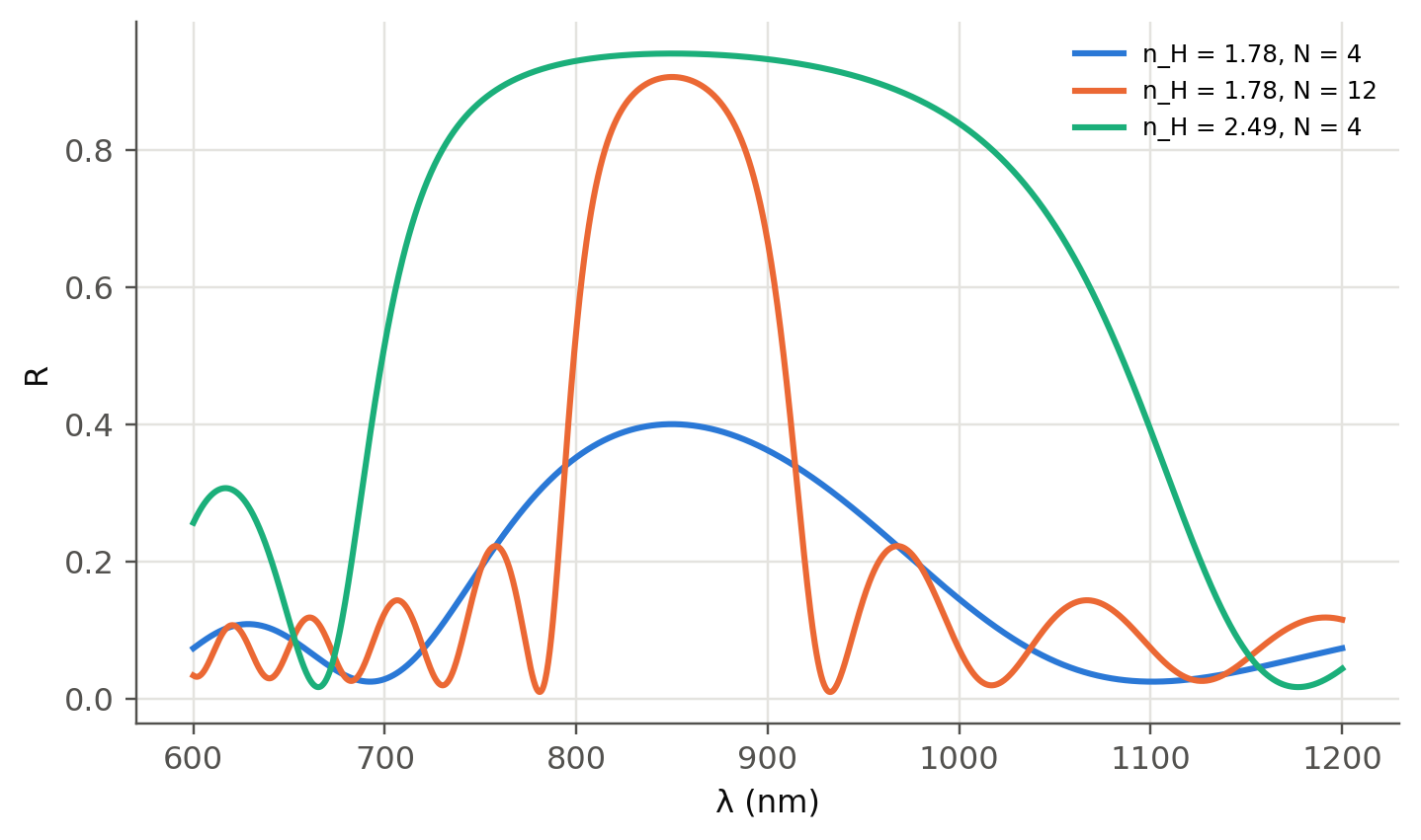
The slides give R₄ = 94.0 % and R₁₂ ≈ 100 % for TiO₂/SiO₂, 80.8 % for the interchanged Ta₂O₅ stack, and Δλ = 74.8 nm for Ta₂O₅/SiO₂.
The Ta₂O₅ values for N = 4 and 12 (40.0 % and 90.6 %) are not printed on the slides but follow from the same formula. The contrast
matters: 4 pairs of TiO₂/SiO₂ do better than 12 pairs of Ta₂O₅/SiO₂.
```{python}
#| label: fig-bragg
#| fig-cap: "Reflectance spectra of the quarter-wave mirrors of slide 185, computed with the transfer-matrix method."
lam = np.linspace(nm(600), nm(1200), 1500)
fig, ax = plt.subplots()
for k, (nH, N) in enumerate(((1.78, 4), (1.78, 12), (2.49, 4))):
    ax.plot(lam*1e9, ol.tmm(*ol.qw_stack(nH, 1.55, N, lam0), lam)[0], color=ol.PALETTE[k], label=f"n_H = {nH}, N = {N}")
ax.set(xlabel="λ (nm)", ylabel="R"); ax.legend(fontsize=8); plt.show()
```
## Worked example: penetration depth of a Bragg mirror (slide 189)
A Bragg mirror reflects as if it were a perfect mirror placed at a distance $L_\text{pen}$ *inside* the stack. This matters for the
effective cavity length of VCSELs. We extract it from the slope of the reflection phase.
```{python}
lam = np.linspace(nm(840), nm(860), 801)
_, _, r = ol.tmm(*ol.qw_stack(2.49, 1.55, 12, lam0), lam)
k = 2*np.pi/lam
phi = np.unwrap(np.angle(r))
Lpen = -0.5*np.gradient(phi, k)[400]
print(f"TiO2/SiO2 12 pairs: L_pen = {Lpen*1e9:.0f} nm  (estimate λ/(4Δn) = {850/(4*(2.49-1.55)):.0f} nm)")
```
## The photonic band gap behind the Bragg mirror (slides 289–294)
For an infinite bilayer lattice of period $\Lambda=d_1+d_2$, Bloch's theorem gives the dispersion relation of the 1D photonic
crystal (slide 292):
$$
\cos(K\Lambda)=\cos(k_1d_1)\cos(k_2d_2)-\tfrac12\left(\tfrac{n_1}{n_2}+\tfrac{n_2}{n_1}\right)\sin(k_1d_1)\sin(k_2d_2).
$$
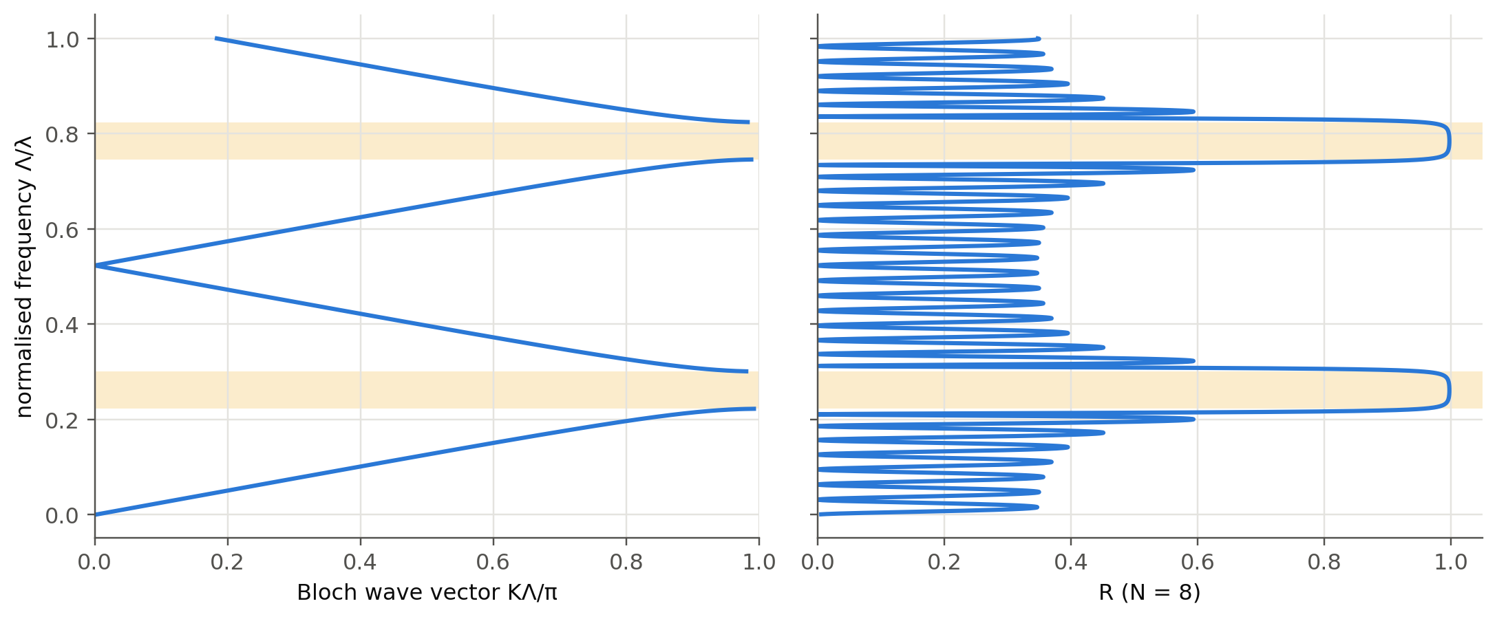
Where the right-hand side exceeds 1 in magnitude, $K$ is complex: no propagating Bloch wave exists, and a finite stack reflects.
```{python}
#| label: fig-bandgap
#| fig-cap: "Left: band diagram of a TiO₂/SiO₂ quarter-wave 1D photonic crystal. Right: reflectance of an 8-period finite stack on the same frequency axis. The shaded bands are the photonic band gaps."
n1, n2, Lam = 2.49, 1.55, 1.0
d1, d2 = Lam*n2/(n1 + n2), Lam*n1/(n1 + n2)     # quarter-wave condition n1 d1 = n2 d2
f = np.linspace(1e-3, 1.0, 3000)                 # normalised frequency Λ/λ
k0 = 2*np.pi*f/Lam
rhs = np.cos(k0*n1*d1)*np.cos(k0*n2*d2) - 0.5*(n1/n2 + n2/n1)*np.sin(k0*n1*d1)*np.sin(k0*n2*d2)
gap = np.abs(rhs) > 1
KL = np.where(gap, np.nan, np.arccos(np.clip(rhs, -1, 1))/np.pi)
R8 = ol.tmm([1.0] + [n1, n2]*8 + [1.0], [d1, d2]*8, Lam/f)[0]
fig, ax = plt.subplots(1, 2, figsize=(10, 4.2), sharey=True)
ax[0].plot(KL, f); ax[0].set(xlabel="Bloch wave vector KΛ/π", ylabel="normalised frequency Λ/λ", xlim=(0, 1))
ax[1].plot(R8, f); ax[1].set(xlabel="R (N = 8)", xlim=(0, 1.05))
idx = np.where(gap)[0]
for blk in np.split(idx, np.where(np.diff(idx) > 1)[0] + 1):
    if blk.size:
        for a in ax: a.axhspan(f[blk[0]], f[blk[-1]], color=ol.PALETTE[3], alpha=0.2, lw=0)
plt.tight_layout(); plt.show()
```
The stop band of the finite stack coincides with the photonic band gap of the infinite crystal, and the index contrast sets the gap
width. The "interference of reflections" picture explains *why* a band gap appears; the Bloch picture gives its *size*. In 2D and
3D (slides 289–293), a full band gap needs a large contrast and the right lattice. Point defects then act as cavities and line
defects as waveguides (slide 294).
## Worked example: a fiber Bragg grating
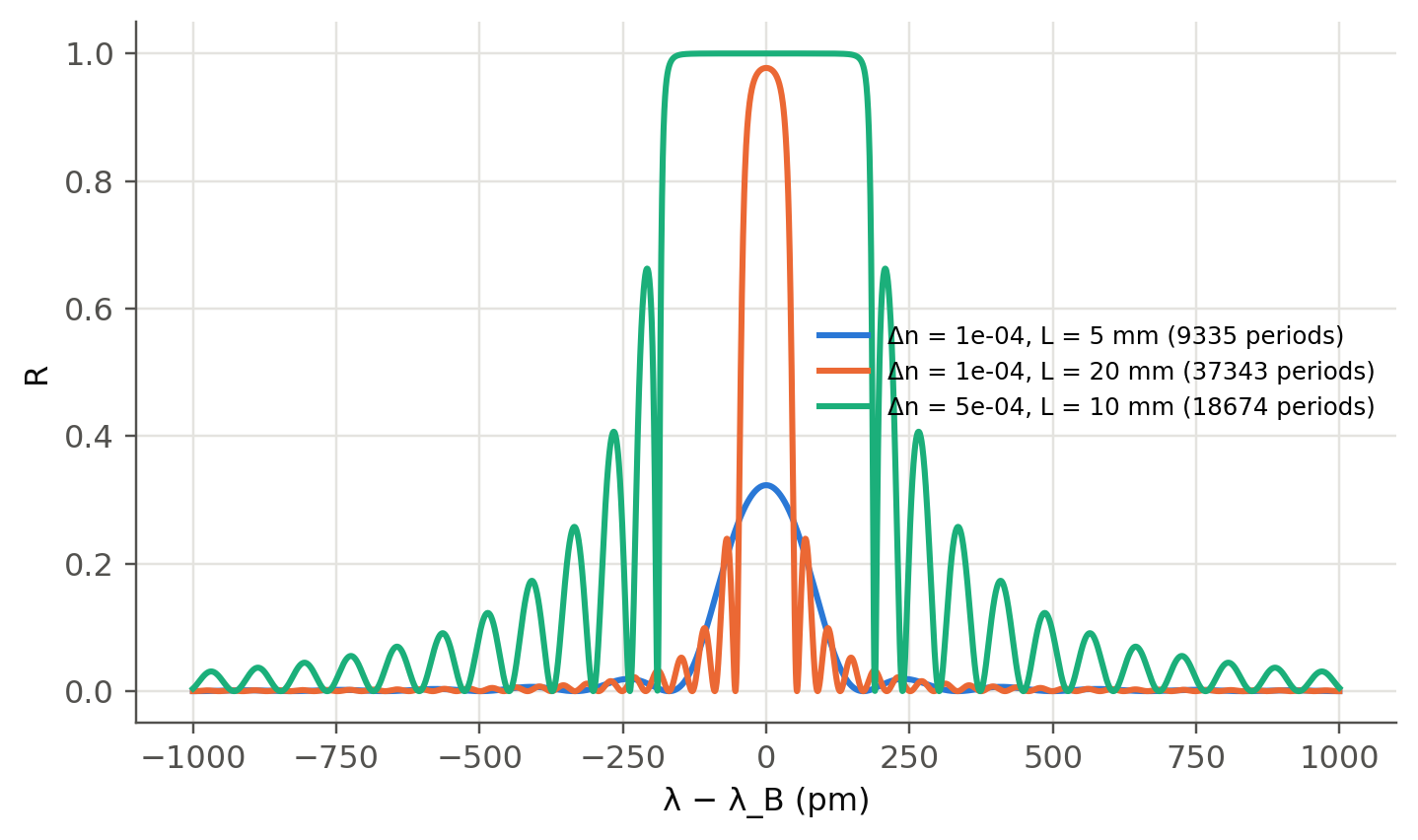
A fiber Bragg grating (FBG) is a Bragg mirror with a tiny index contrast ($\Delta n\sim10^{-4}$) but tens of thousands of periods.
The same transfer-matrix approach applies; Chapter 2 treats FBGs in detail (coupled-mode theory, apodisation, sensing).
```{python}
#| label: fig-fbg
#| fig-cap: "Reflectance of uniform fiber Bragg gratings computed as Bragg stacks with tens of thousands of periods (matrix power of the unit cell)."
def periodic_R(n0, na, nb, da, db, N, ns, lam):
    def layer(n, d):
        dl = 2*np.pi*n*d/lam
        M = np.empty((lam.size, 2, 2), complex)
        M[:, 0, 0] = np.cos(dl); M[:, 0, 1] = 1j*np.sin(dl)/n
        M[:, 1, 0] = 1j*n*np.sin(dl); M[:, 1, 1] = np.cos(dl)
        return M
    M = np.linalg.matrix_power(layer(na, da) @ layer(nb, db), N)
    B = M[:, 0, 0] + M[:, 0, 1]*ns; C = M[:, 1, 0] + M[:, 1, 1]*ns
    return np.abs((n0*B - C)/(n0*B + C))**2

neff, lamB = 1.447, nm(1550)
lam = np.linspace(nm(1549.0), nm(1551.0), 3000)
fig, ax = plt.subplots()
for dn, Lg in ((1e-4, 5e-3), (1e-4, 20e-3), (5e-4, 10e-3)):
    na, nb = neff, neff + dn
    da, db = lamB/(4*na), lamB/(4*nb)
    N = int(Lg/(da + db))
    ax.plot((lam - lamB)*1e12, periodic_R(neff, na, nb, da, db, N, neff, lam),
            label=f"Δn = {dn:.0e}, L = {Lg*1e3:.0f} mm ({N} periods)")
ax.set(xlabel="λ − λ_B (pm)", ylabel="R"); ax.legend(fontsize=8); plt.show()
```
::: {.callout-tip collapse="true"}
## Going deeper
- Omnidirectional reflectors: with enough contrast, a 1D crystal reflects all angles and polarisations in a band (Fink *et al.*,
*Science* 282, 1679 (1998)). Check with `ol.tmm` at oblique incidence.
- Coupled-mode theory: derive $R=\tanh^2(\kappa L)$ and compare with the transfer-matrix result for the FBG.
- 2D/3D photonic crystals require plane-wave expansion (MPB) or FDTD (Meep). A point defect is a cavity; a line defect is a waveguide
with slow light (@sec-group).
- VCSELs (Chapter 4) use two Bragg mirrors with $R>99\,\%$. Count the AlGaAs/GaAs pairs needed ($n\approx3.0/3.5$).
:::
::: {.callout-note collapse="true"}
## Complements
- J. D. Joannopoulos, S. G. Johnson, J. N. Winn, R. D. Meade, *Photonic Crystals: Molding the Flow of Light*, 2nd ed., Princeton
(freely available from the authors' website).
- A. Yariv, P. Yeh, *Photonics: Optical Electronics in Modern Communications*: periodic media and coupled-mode theory.
- R. Kashyap, *Fiber Bragg Gratings*.
:::
## Try it yourself
1. With the live panel, find how many TiO₂/SiO₂ pairs give $R>99.9\,\%$. Why does a metal mirror (95–98 %) lose this race (slide 190)?
2. Shift the design wavelength while keeping the layers fixed: this is how a Bragg mirror is "tuned" by temperature or strain.
3. Put a half-wave spacer between two Bragg mirrors with `ol.tmm`. What appears at the centre of the stop band? (This is the cavity
of @sec-fp.)